
Epitaxial silicon detectors
kordyasz@nov.slcj.uw.edu.pl
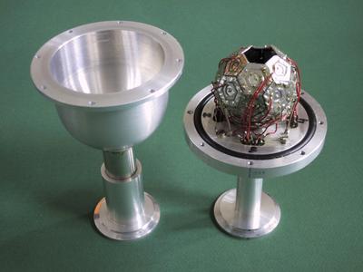
Figure 1. Silicon ball.
2. Thin (65 μm), large area (64 cm2) epitaxial detectors on thick silicon layer with electric field build in have been produced. The detectors were used to assemble the set-up to:
- measurement of radon concentration in environmental water [2],
- measurement of radon emanation from solids [2],
- measurement of 224Ra and 226Ra concentration in environmental water [3],
- measurement of environmental aerosols radioactivity and αradioactive surface contamination.
The setup has been also used for nuclear physics didactic. 3. A new technology named PPPP (Planar Process Partially Performed on the Thin, Silicon Membrane) [4,5] has been elaborated and necessary devices were constructed. Using this method a passivated 52 μm thick transmission ΔE strip detector (Fig.2) was produced . During tests the detector was able to resolve light charged particles p, d, t, α from 9B(p,X) reaction and He, Li, Be, B from 9B(14N,X) reaction (Fig. 3). Very thin (1.3, 2.5, 3.2, 4.3 μm) transmission detectors were also manufactured and tested.
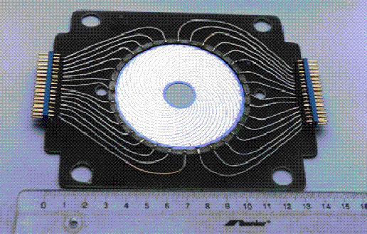
Figure 2. The passivated 52 μm thick transsmision ΔE strip detector.
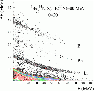
Figure 3. E-ΔE contour plot obtained after irradiation with α particles and medium heavy ions Li, Be, B of the telescope with 52 μm thick ΔE detector followed by 400 μm thick E detector.
4. A new technology named Quasi Selective Epitaxy [6], based on well-known selective epitaxy, has been developed. Using this method two monolithic E-ΔE telescopes were produced:
- with ΔE transmition detector 20 μm thick, that was able to resolve hyperbolas of He, Li, Be, B, C, N, O, F and Ne (Fig. 4a)
- with ΔE transmition detector 4 μm thick, dedicated to fission products registration (Fig. 4b)
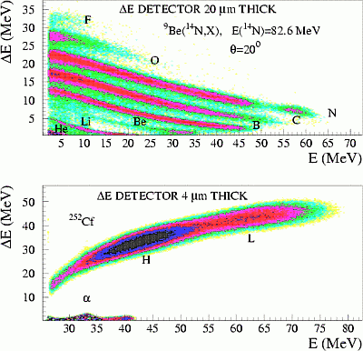
Figure 4. a) E-ΔE scatter plot obtained after irradiation with heavy ions of the monolithic E-ΔE telescope with 20 μm thick ΔE detector b) E-ΔE scatter plot obtained after irradiation with fission fragments and α particles from 252Cf source of the monolithic E-ΔE telescope with 4 μm thick ΔE detector. L-light fission products H- heavy fission products.
5. An epitaxial, silicon, planar , mosaic detector, which can be used for the particle detection in Coulomb excitation experiments, has been constructed and tested. The mosaic detector is a semiconductor segmented device, consisting of 35 segments made on the 3 inch wafer.
Bibliography
[1] The 4 π epitaxial Si detectors array for in-beam spectroscopy experiments A. Kordyasz et al.,Nucl. Instr. and Meth A 390 (1997) 198
[2] Measurements of radon activity in water and radon emanation from solids, A.J. Kordyasz et al.,
Proccedings of the European Conference on Advances in Nuclear Physics and Related Areas, Tessaloniki, Grece 8-12 July (1997) 878
[3] Simultaneous Determination of 224Ra and 226Ra Isotopes by Measuring of Emanated 220Rn and 222Rn Using a 4-Inch Silicon Epitaxial Detector,
A.J. Kordyasz, B. Bartos, A. Bilewicz, Chem. Anal. (Warsaw) 49 (2004) 29
[4] Silicon passivated thin ΔE strip detectors produced using the PPPP process A.J. Kordyasz et al.,
Nucl. Instr. and Meth. Reg. No.: KNO 4 544 (in print)
[5] Silicon passivated thin ΔE strip detectors produced using the PPPP process A. Kordyasz et al.,
Warsaw University Heavy Ion Laboratory Annual Report (2003) 37
[6] Monolithic silicon E-ΔE telescope produced by the Quasi-Selective Epitaxy A.J. Kordyasz et al.,
Nucl. Instr. and Meth. A 528 (2004) 721